-
Etching your own PCBs
 Disclaimer:- I’m not claiming this is the best way to make PCBs, its just what I do (for one-off, simple boards) – and it works well more often than not. Also, the chemicals involved are pretty nasty so due care should be taken.. etc.. etc..
Requirements:
For drawing / printing the actual PCB layout:
- A dedicated CAD program or simple art package.
- An inkjet or laser printer
- Compatible transparency film sheets.
- A UV exposure box (expensive*)
- Pre-sensitized copper clad board.
- Optional: Tin-plating crystals
(* Around £80+ but can be hand built cheaper EG: Buy some spare UV tubes, a starter and ballast unit from a place that sells the light boxes. The tubes used in PCB exposure units use lower frequency radiation than those used in EPROM erasure units and therefore should be safer to work with (EPROM erasure UV tubes are EXTREMELY hazardous to the eyes and should absolutely not be used). Avoid exposure to the UV light anyway – if in doubt, bite the bullet and buy a ready made unit or use an alternative production method – better safe than sorry).
For developing the board:
- Sodium Hydroxide (Caustic Soda crystals)
- A plastic tray.
- Water, cold (or tepid at most – definately not hot or even warm)
- A pair of plastic tweezers (for getting the the board out of the chemicals without using your fingers!)
For etching the board.- Ferric Chloride (crystals or ready made solution.)
- Water – hot, but not boiling.
- A small tray, slightly bigger than your PCB is ideal.
For drilling..
- Ideally, a bench-mounted vertical drilling machine of some sort.
- A drill bit of 0.75mm diameter for most holes (0.9mm for pin headers etc.)
In brief, the process is:
- Draw circuit on PC.
- Print circuit onto transparency film to make a positive mask.
- Place mask against photo-resist coated copper blank PCB and expose to UV.
- Develop PCB in sodium hydroxide solution (removes coating where UV has been absorbed)
- Etch PCB in Ferric Chloride solution (actually removes the unwanted copper)
- Remove remaining photo-resist coating.
- (Optional: Tin plate)
- Drill.
- Solder components
There are quite a few variations on this basic process, eg: for a simple one-off circuit you can use rub-down track transfers directly onto an uncoated copper board, or used special iron-on transfer sheets to transfer a more complicated design (which is described here). Personally, I do it the “long way” outlined above..
In detail..
1. Drawing..
There are CAD programs available to automate the layout process, most of them are commerical, very expensive or linked to PCB production companies that manufacture the boards for you. There are however a few decent free programs such as FreePCB and Eagle (which even has an auto-router – but is limited to 4″ x 3″ PCBs in the demo version). Both programs generate Gerber files (for professional PCB production) and FreePCB will also output .png versions for direct home printing + etching. I’d now recommend using FreePCB, but of course you can also draw PCB designs by hand in a simple paint program – I’ve used this approach a lot myself in the past so I’ll describe it below before describing the actual etching process:
Hand-drawn PCBs..
A resolution of 180dpi (which is an even fraction of my printer’s native resolution of 1440dpi) is sufficient for simple circuits (I have sucessfully used upto 720 dpi for the 0.5mm pin pitch of QFP SMT devices – though that’s really pushing it:). “Through-hole” components generally have a pin spacing of 0.1″ (or multiples thereof) so that means 18 pixels between hole centres. I find the smallest details I can get away with at this resolution are tracks 4 pixels wide with spaces of 2 pixels between them. Make sure your pad holes are of adequate size else you’ll have trouble finding the centres when drilling (a circle of 4 pixels diameter is ideal at this resolution).
Starting off with a pre-prepared image template (a grid of DIL pads drawn in grey) I colour the required pads black and join them up as per the circuit. I draw my circuits from the components side as if looking down at the tracks through a PCB made of glass – its effectively a mirror image of what you’ll see when looking at the back (track side) of the completed PCB. (There’s no need to mirror it when printing either as you want the printed side against the PCB blank to get the sharpest mask.) Sometimes it’s useful to “add a new layer” in PSP and set it at 50% transparency, on this you can draw on the actual components to check for spacing etc (the grid function of PSP often comes in handy too.) When complete, remove any grey pads from the image either with the selection tool plus “select similar” or by adjusting the image contrast until I pure black on a white background (naturally you’ll need to remove any added image layers too). If you find you have a lot of large white areas it’s desirable to fill these in with the rectangle tool (being careful not to short anything) as it’ll mean less copper to remove when etching. Here’s an example of one of my PCB designs.
2.Printing…
You need to print the design on a transparency sheets rather than any kind of paper so that the UV can pass through the clear bits well enough to give a good exposure. You can use inkjet (or laser as applic.) OHP transparencies but depending on the results you may need to print the image twice, cut them out and and overlay the two patterns exactly to give a satifactory mask. (I originally had excellent results with “Jetstar Standard” Inkjet film from Mega Electronics but they seem to have changed the coating quality recently to something less impressive – its still better than OHP sheets though). Anyway, you will probably have to experiment with your printer settings to get the best results. (“Photopaper” / “photo quality” seems about right on my Epson C84 – if there’s ink pooling, you’ll need to crank it down a shade. Conversely, if the mask is not solid enough or streaky, turn it up). Naturally you must ensure your printing is exactly 100% full-scale.
3.UV Exposure..
Make sure your printed mask has dried (else it’ll stick to the UV coating on the PCB and ruin it) and peel the protective layer off the presensitized PCB blank. Place your transparency with the printed side against the copper coating and put the two face down in the light box, close the lid, switch on and allow 6-7 minutes exposure time (a little longer, say 30 seconds, may not harm things too much if its a good dark mask but you may get a dilated exposure which can ruin things if the tracks are thin). Experimentation with small pieces of board can save frustration. When the exposure time is up, switch off the UV light and remove the PCB – you may not see any visible change in the coating at this point – that’s normal. (If you’re not ready to develop it immediately, keep the PCB in the dark.)
4. Developing..

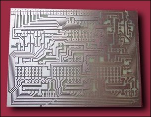
Photoresist after developing
The developing solution is just sodium hydroxide (caustic soda) crystals dissolved in cold (about 20’c) water – see the note about concentration below. You need about half a litre of solution poured into a plastic tray – I normally prepare this whilst the PCB is being exposed in the UV box. You simply place your UV-exposed PCB in the developing solution and rock the tray gently for a few minutes (try to do the developing out of direct bright sunlight – I’ve found it can expose the coating as it develops if the process starts taking some time). Within a few minutes you should see your circuit stand out dark and the exposed coating wash away. Make sure the process is complete before removing the PCB from the tray – the copper should be shiny pink against the dark track layout. If things arent happening – you can speed up development with a little more agitation, or by adding some warm water or a small amount of stronger solution. Try to be patient as often it’ll get there in the end and too strong/warm a solution will just strip everything from the board. If the result was a total disaster you will have adjust one of the parameters, more/less time in the UV box, weaker/stronger or warmer/cooler solution. Assuming it came out OK, extract the PCB using a pair of tweezers and give it a rinse under the cold water tap. When you’re finished this part you can pour the sodium hydoxide solution straight down the sink, but remember wash it down well to prevent anyone getting splashes etc (although it just feels soapy, sodium hydroxide solution is quite nasty so be careful). There are safer, more efficient developing solutions available too (see “suppliers”) – they cost more though, of course..
Note: The concentration of the developer varies depending on the make of photoresist PCB – For example Maplin’s PCBs need a solution strong enough to strip *everything* off PCBs supplied by Rapid and ESR (IE: “Photoboard 2”). Try to get a datasheet or failing that, start off with a weak solution (1 teaspoon of crystals to a litre of water), give it a couple of minutes and if nothing much is happening add small amounts of stronger solution (Dont be tempted to add crystals directly to the tray with the board in it, they wont dissolve quick enough and the concentrated crystals will ruin the board)..
5.Etching..
Now for the really nasty stuff: Ferric Chloride (chemical name FeCl3). This is the acid that is used to etch away copper that isn’t protected by the remaining photoresist coating (it also stains things like crazy so wear old clothes and plastic gloves when going anywhere near it!) FeCl3 often comes in bags in its anhydrous from (dried orange-brown coloured crystals) but you can get ready made solution too. Again, there are more expensive/friendlier/cleaner substitutes. If making up your own solution, you need about 100 grams of crystals per 200ml of water – but it’s not at all critical. Place the crystals in a small plastic tray and slowly add some hot (40’c) water – you dont need more than 1cm’s depth. Gently rock the tray to disolve the crystals and only when they’ve completely disolved, place the PCB in. Etching should take less than 20 minutes, especially if the solution stays warm and you agitiate the tray gently.
Use plastic tweezers to observe the PCB occasionally, obviously its easy to tell when its complete – you dont want to leave it in the solution too long as the FeCl3 will start to ingress into your tracks. Wash the PCB thoroughly when done. When you’ve finished with the Ferric Chloride solutionn you can either store it for later use (assuming it has any etching power left) or dispose of it safely – I would not recommend putting this stuff down the sink!!
6. Cleaning..
First clean off the remaining UV coating. One way to do that is to expose the PCB to UV again (obviously without any mask) and then put back it in sodium hydroxide solution for a while (or skip the UV part and just put it in some stronger Sodium Hydroxide solution – not too strong though or the copper will go black). Alternatively, you can just use a cleaning solvent such as isopropol alcohol or a small polishing block / brillo pad.

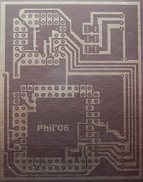
Example of tinned PCB
7. Protecting (Optional stage – tin plating).
Freshly etched copper tracks oxidise quite quickly and this can cause problems when soldering. Ideally its best to protect the copper somehow if you’re not going to be soldering relatively soon. Obviously the simplest thing to do is leave the photoresist mask on until you’re ready to solder. Or you can paint the copper tracks with a flux pen, it’ll dry quite quickly to form a coating that protects the copper until soldering at which time it’ll melt, helping make a good joint.
Alternatively, you can plate the exposed copper using tin plating crystals (EG: available from Rapid Electronics in the UK) This is a simple process (if somewhat expensive): Just mix the crystals with hot tap water (50’C), leave to cool to room temperature, clean PCB thoroughly, rinse it and then immerse it in the solution for 30 minutes. The mixed solution lasts about 6 months, the crystals have an unlimited shelf life.
8. Drilling..
Ordinary power drills are definately out! You need something that will be accurate – a bench drilling machine is ideal but you can get small hobby drills (Dremmel style) that’ll sit in a frame of some sort to keep them vertical. If the chuck doesn’t take the tiny drill sizes you may be able to buy a “pin-chuck” or get reduced shank drill bits (recommended). Place a flat piece of wood under the PCB, use an appropiate speed setting and dont go bull at a gate or you’ll end up breaking lots of drill bits :)
A note about non-PCB metal etching:
The techniques above can be used to etch other metals such as brass and stainless steel for craft, modelling purposes etc. The big difference is that you’ll need to apply a photo-resist coating to the clean bare metal yourself (if using the UV exposure method). This chemical is available in spray form and also as an applicator (EG: “Seno Positiv 100” available from Rapid Electronics in the UK). Coating the metal is a little bit of challenge – the “paint” needs to be applied evenly, in subdued light, in a dust-free environment and left to dry in the dark. I found the Seno applicator the least hassle – it dries quickly (10 mins, with 5 hours optimum) and its less prone to dust pickup than spraying. It is also possible to buy photoresist in sheets, which have to be pressed onto the bare metal – you can find these on ebay often from Chinese suppliers. Note: With this method, you usually need to make a negative mask and will need to use the appropriate developer (IE: not the usual sodium hydroxide).
UK Suppliers:
- ultravioletexposureunits.co.uk
- Rapid Electronics
- Maplin Electronics
- ESR Electronics
- Mega Electronics

