-
CPLD intro
As I found out with my Z80 project, designs based on discrete logic ICs can soon sprawl across many PCBs. As well as the physical space taken, this leads to issues with signal integrity, noise, capacitance etc. Fortunately user-customisable chips (CPLDs and FPGAs) which provide the same functionality as many logic ICs are now quite accessible even for hobbiests. There are two main differences between the two groups, CPLDs (Complex Programmable Logic Devices) are flash-programmable and small scale in nature, FPGAs (Field Programmable Gate Arrays) are generally much more complex and based on SRAM (so do not hold their configuration pattern after a power down). When reworking my Z80 project I chose to use CPLDs – I knew I’d need multiple chips (one FPGA would hold the entire project) but I didnt want to try to “run before I could walk” so kept things as simple as possible.
Quite a few companies now make these types of chips but the major players seem to be Xilinx and Altera, both of whom make a range of CPLDs and supply free development software. Its also a fast paced area of electronics and the newest devices from all companies are aimed at 3.3 volt and lower logic and only come in high pin density, non-socketable packages. At the time of writing, Xilinx’s older XC9500 series CPLDs are available. These are single supply 5 volt parts available in PLCC format which made prototyping easier. I bought some chips from that range (namely the XC9536, XC9572 and XC95108) via Digikey.com. The XC9536 is the smallest being a 44 pin device with 36 macrocells, the XC9572 and XC95108 are 84 pin devices with 72 and 108 macrocells respectively. One macrocell is a small block of customizable logic which can configured to perform certain functions. EG: a flip-flop may take up one macrocell, and so might a 2-to-1 AND/OR selector. Capacity is generally measured in these macrocells rather than individual gates because of the way the chips are internally structured. As mentioned, the software used to enter the logic circuits was a free download from the Xilinx site – I used “Xilinx Webpack ISE 7.1” at the time. The software package allows designs to be entered using schematics (wired up logic symbols) or via text with a high level “behaviorial” language such as “Verilog”. Each method has its own advantages – schematics alone are simplest but unwieldy for really big projects. But then learning a whole new and abstact language for a hobby project might not be your idea of fun electronics. Personally I was fine with the schematics, despite the development software being pretty unstable on my PC. (Tip: Save work regularly!:) A logic simulator (a cut down version of “Modelsim”) was also available seperately at the Xilinx site (now integrated into the newer Webpack editions) and allows designs to be tested before flashing them onto chips.
The great thing about CPLDs is that once you’ve entered your design, you can assign the physical pins to your signals pretty much willy nilly. This obviously makes PCB layout easier as you can place tracks based on the shortest route or whatever. Sometimes there will be a macrocell usage penalty by setting your own constraints but its really quite flexible. (You can just let the software chose the pins automatically if you wish).
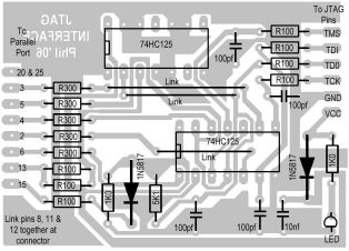
Actually burning the design to the chip is easy – the software to do so is part of the development package. The hardware required to program older ranges of CPLD/FPGA such as the XC95xx(XL) series of CPLD and Spartan2 series of FPGAs can be made up yourself. In fact Xilinx provide a schematic for their Parallel3 JTAG interface lead – (click pic above for an archive with PCB mask, parts list etc of such an interface I made). To program the newer ranges of chips, a more modern USB lead is available from Xilinx.
Issues:
- Output levels – I was using CPLDs to replace 5 volt 74HC logic, however the Xilinx XC95xx CPLD IOs are stated in the datasheets as only being TTL level compatible. The outputs are not fully CMOS compatible, offering a logic high of around 4 volts. Still, the threshold of 74HC part is about 3.5 volts so they SHOULD interface directly. Personally I didn’t take any chances so changed to 74HCT ICs where I still had to use discrete logic. Other workarounds include raising the CPLD’s Vcc to 5.5v or using pull-up resistors.
- Ground bounce – as with most logic ICs when lots of outputs switch simultaneously a noise pulse can be injected into supposedly stable outputs. This can cause major problems if one of the affected outputs is driving a clock line. Ground bounce effects can be minimized on the CPLDs by various methods:
- Staggering output switching times (the “BUF” symbol can be used to delay outputs, but make sure an attribute “OPT” is set “OFF” else it’ll normally be removed during compilation)
- Setting the pin slew rates to “slow”
- Having good ground connections to the chip
- decoupling capacitors across the supply close to the VCC pins.
- Tying unused IO pins to ground, setting them to “Programmable Ground” in the options.
- Solder the part direct to the PCB, rather than using sockets
Links / Further Reading:
The One Hour Xilinx Design Challenge
Parallel 3 Programming Cable Schematic


