-
Z80 Project – The Early Years
[Edit] On request I’ve resurrected this old article – it describes the construction of my first Z80 projects based on discrete logic and microcontrollers (it’s a lot easier with CPLD/FPGAs – though the raw chips are physically not as hobbyist friendly – a dev board is the best bet if you want to design your architecture “virtually”) Saying that, modern microcontrollers such as the Propellor are a lot more powerful than what I was playing around with…) Anyway, here goes:
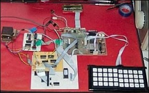
My first attempt at a complete Z80-based computer system was a sprawling mass of boards and cables and very limited with it. It had only a membrane keyboard and 8×8 grid of LEDs for the display (Pong never looked so err…primative) Still, it was interesting to tinker with and set me off on the road to better things.. One such thing was my own graphics “card” – I wanted to connect the project to a TV and have a proper display. Unfortunately, I didn’t really have the technical knowledge at the time, so for that and other reasons the Z80 project gathered dust…
Fast forward about a decade (!) and with the power of the Internet at a geek’s fingertips, obtaining technical information was no longer a problem. After a bit of browsing I soon embarked on my version 2 Z80 Project.
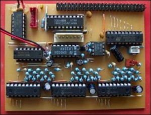
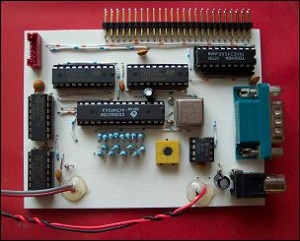
The V2’s Z80 Mainboard’s Ingredients:
One 8MHz CMOS Zilog Z80 CPU
One 8KB EPROM (120ns) mapped in at $0000-$1FFF
One 8KB SRAM (70ns), mapped in at $4000
One 128KB SRAM (70ns), mapped into $8000-$FFFF as four switched banks of 32KB.A 74HC139 dual demultiplexor IC used in conjunction with a 74HC32 (quad OR) chip to create read/write enable signals for ports 0-3. All but the signals for Port 0 are routed off board via external connectors.
A 74HC245 buffer to handle input from Port 0 (Such as the project’s individual IRQ status lines, serial data/clock in, onboard button status..)
A 74HC574 latch to hold bit settings for Port 0. (Such lines as the 32KB bank select (ie: 128KB SRAM address lines A15 and A16), onboard LED indicator, piezo buzzer, serial comms data/clock out.
A 74HC14 (hex inverter) and a 74HC32 (quad OR) to merge the incoming interrupt lines into the Z80’s single IRQ source and also to handle some of the memory select decoding.
Two small push buttons; one to reset the Z80 (via a resistor/capacitor time delay driving a Schmitt inverter gate) and the other to act as simple input line (which I used for testing before the keyboard interface was developed).
Finally, for general testing there’s an LED and PCB-mounted piezo buzzer which are driven by the 574 latch IC via resistors.
Some Notes:
The Z80’s NMI line is just pulled high via a resistor. I guess I could’ve connected this to an unused output on the keyboard controller PIC in order to enable a freeze-button type feature.
The Z80’s /BUSREQ line is also pulled high as my project didn’t need any DMA to the system bus.
The Z80’s 8MHz clock signal is derived externally from the 64Mhz video clock.
The video system:
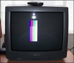
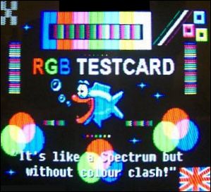
Starting out, I found this website particularly useful – Rickard produced TV output (and games) using a single PIC 16C84 microcontroller. I’d used PICs myself a lot in the past so I wrote some quick test code to produce a stable TV signal using Rickard’s info as a template. At first I only sent signals to the composite video line, this allows a grey scale image to be produced with a slowish microcontroller. Colour via composite needs a faster microcontroller and I didnt have any at the time so I tried using 3 ports from the PIC to control the TV’s SCART RGB lines instead – see pic. (I’ve put together a simple demo circuit based on a PIC 16F628. The code is quite easy to follow as it doesn’t do much except create the timing frame and show some colour bars. Download code/schematic here )
Unfortunately even in RGB mode, the PIC 16C84/16F84 (and more recent 16F62x) range of microcontrollers were too slow to produce video at a decent horizontal resolution on their own. With a 5Mhz instruction clock (20Mhz source clock) the pixel size would be almost four times that of a Sinclair ZX Spectrum (each pixel needs 2 instructions, a read and write instruction – limiting the pixel clock to 2.5Mhz). Also the PICs I was using didnt have enough ports to be able to fetch data from external memory without a lot external latching which would slow things down even more.
So at this point I decided to use the microcontroller just to provide the TV timing “framework” and design the serious bit of the graphics board using discrete logic ICs. I reckoned a 256×192 pixel display would serve my purposes so I modified the PIC RGB test code to produce an appropriate display window. This is basically what it does to create my display window within a non-interlaced 312-line PAL TV frame:
Do 56 blank lines (y border)
Do 192 display window lines (x-border, display, x-border)
Do 56 blank lines (y border)
Do special vertical sync lines (reset TV’s raster beam)
LoopSome detail:
“Blank line” – 4uS sync low pulse, 60 uS delay..
“Display Window Line” – 4uS sync pulse, 18 us delay, 32 uS display window (256 pixels), 10 us delay..
“Vsync Lines” – For a non-interlaced display: 6 equalizing syncs, 5 long syncs, 5 equalizing syncs (see this page for details).
With the PIC microcontroller handling the TV timing, I planned out the other features of my graphics system. It was always going to be a bit-mapped display and I didn’t want any horrendous Spectrum-like colour attributes. The simplest design would have been to fetch a byte for each pixel from an SRAM chip and use bits from that byte to drive the TV’s RGB lines on or off. As well as being wasteful of memory, such a system would also limit to the display to 8 colours (the primary and secondary colours). Instead, pairs of bits could be fed to 3 digital to analogue converters: More colour resolution, less wasteful and 64 colours on screen. However, with one byte per pixel, even my 256×192 display would take 48K, slightly too much of the poor Z80’s address space! Bank switching could be implemented but that would’ve made access to the screen less straightforward. Anyway, the main reason this system wasn’t used was the sheer amount of data the Z80 processor would have to shift in order to move anything around the screen – it just isn’t up to that kind of workload.
In the end I went for an Amiga-like bitplane (planar) system. In my design, several monochrome bitmap pages (pretty much a Spectrum’s display each, less attributes) are stacked “on top of” each other, and each pixel is created by combining the bits (one from each page) into a “pixel word” which has a bitlength dependant on the number of bitplanes used. Each bitplane would only take (32 bytes x 192) = 6KB and only one bitplane really needs to be mapped into Z80 address space at any one time. The CPU workload is also reduced because the CPU doesn’t have to write to all the bitplanes if less colours are involved in an operation. The downside to this system is that it does complicate the design – each pixel has to be constructed from bytes at separate locations in memory, shifted and combined. More on this later.
A 3-bitplane system with each bit directly controlling the R,G,B lines would make a simple circuit on the TV output side: As each line is either on or off no digital to analogue converter is required, just a single resistor on each line to drop the logic-level voltages down to 0.7 and 0 volts respectively. However, I wanted a colour palette with up to 16 colours on screen – so I specified 4 bitplanes and sent the 4-bit pixel word from the bitplane combination logic to the address lines of a small (and reasonably fast) SRAM chip which holds the palette data.
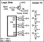
The palette SRAM produces a whole byte for each pixel but as 8 bits doesn’t divide nicely between the three Red, Green & Blue channels I originally just ignored the top 2 bits and allocated 2 bits per channel giving 4 brightness levels for each colour component. To get the binary values to produce analogue voltages between the RGB-spec 0v and 0.7v I used 2 resistors per channel, a 750 ohm resitor on the MSB and a 1500 ohm resistor on the LSB. The other ends of the resistor pairs are connected together and sent to the TV’s RGB lines via the SCART socket. As the TV effectively has 75 Ohm resistors to ground on each line, a potential divider is created that sets the correct voltage levels. This system gave a palette of 64 colours.
I later improved this slightly using bits 6 and 7 from the palette SRAM output to give greater colour resolution on the Red and Green lines, simply by connecting them via 3000 Ohm resistors to the scart lines. There obviously wasn’t a 9th bit for the Blue line so that had to stay at 2-bit resolution. The output circuit is shown in the pic (the outputs are shown buffered by a 74HC574 latch IC). The composite sync line is also shown: 5 volts from the logic is buffered by the 10K resistor into a general purpose NPN transistor (emerging at about 4.3v because of the base-emitter voltage drop) and meets a potential divider formed by the 1K Ohm resistor at the emitter and the 75 Ohm resistor in the TV. 4.3v / (1000+75) * 75 = 0.3V – which is the level the TV requires for a “sync Inactive” signal (drops to zero volts for Active). The picture quality is perfectly fine even with simple R2R DAC affair – though I did have to keep the video ground trace seperate from the rest of the logic and route it the main supply “ahead” of the other PCBs to avoid on screen noise patterns.
Going back to the overall graphic system design, it occurred to me that it’d be quite trivial to implement hardware scrolling (a 0-to-7 pixel offset of the display window which saves the CPU having to shift bits manually). For vertical scrolling its just a case of skipping 0 to 7 lines at the top of the frame and for horizontal scrolling it just means delaying the output of each scan line by “x” pixel clock periods.
Now hardware scrolling isn’t that much use unless you have a spare display buffer to build the new image (whilst the hardware scroll does the fine pixel scrolling). A second display buffer was therefore specified in my design – this could also allow the Z80 to access one bank of video RAM at full speed whilst the video controller was reading pixels from the other.
Another useful feature would be video-sync’d interrupts. With Commodore 64 style raster IRQs I could change the colour palette mid screen, do split screen scrolling and so on. I figured such a system would just require a scanline counter set at the beginning of each frame (or anytime afterwards) which would trigger the interrupt when it reached zero.
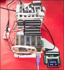
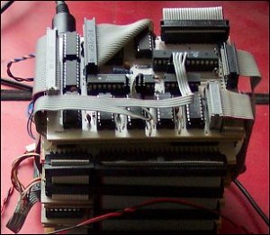
At this point my graphics system ended up consisting of five home-etched (single layer) seperate 100x75mm PCBs stacked on top of each other. I used right-angled pin headers and 50-pin IDC (SCSI) cables and leads to connect them all together to a common bus in a reasonably tidy way (in the cable I alternated every real signal with a ground line to help minimise signal noise). Here’s a brief outline of their functions from a more technical point of view:
PCB 1: Main video controller.. This board coordinates the TV display timing (generates syncs etc) and merges the 4 bitplanes fetched from the VRAM board(s) into a 4 bit nybble for each pixel to send to the palette PCB (four latching parallel to serial shift register ICs (74HC597) handle that). The video controller was orignally based around a PIC16F628 with external counter ICs for hardware scroll etc but now uses an SX28 at 32MHz to perform the same functions in software. The entire system’s master clock is a 64MHz quartz oscillator module whose output is fed directly to the sprite PCB (which has an SX28 running at 64MHz), via a 74HC4024 counter/divider IC to the video controller SX28 (32MHz) and off-board to the Z80 CPU (8Mhz). The SX28 (still) doesn’t actually read in or process the video data itself – it just coordinates everything. Some signals it produces are only required locally, for example the shift clock to the four parallel-to-serial shift regsiter ICs. Other signals are used throughout the system (EG:X-mask, Y-mask (TV border periods) Sync for TV, Vertical Retrace etc). My SX28 source code for the video controller is here.
A video address bus is formed by the output of two 74HC4040 counter ICs plus several bits direct from the SX28. Three such bits are the 3 LSBs of the scanline number -I made those directly controllable for the vertical hardware scroll – they can be set to a 0-7 line offset at the start of the frame and incremented each line down. The MSB of these three is fed to the clock input of the upper 74HC4040 IC so when the count wraps, it increments the “coarse” video address.
The lowest 5 bits of other 74HC4040 IC hold the X-direction byte count (0-31) as the raster sweeps the screen horizontally, it is clocked by output 7 of a 74HC4017 decade counter. The sequential outputs of this IC are used to latch data from four bit-planes into the 74HC597 parallel-to-serial shift registers (each bitplane is addressed by the SX as it controls Video Address lines A13-A14 directly). The only other component is a 74HC157 data selector IC which channels the outputs of the X or Y hardware scroll latches to the SX28 (I ran out of SX input ports, so multiplexed these two 3-bit values).
PCB 2: Palette and output PCB. A small SRAM chip holds the palette table. Two 74HC157 IC switch its address bus between the Z80 (write only) and the video controller (read only). To keep things simple the palette can only be updated when the raster is off screen (either horizontal or vertical masking periods). The first 4 bits of the palette SRAM’s address bus come from the video controller, the 2nd 4 bits from the output of the sprite controller, the other address lines are held low. The SRAM’s data bus is directed to a either a 74HC574 latch (who’s outputs are connected to resistors to form 3 DACs for the red, green and blue lines) or the Z80’s data bus through a 74HC245 buffer IC for palette updates.
PCB 3: Video RAM board 1 (Buffer 0).. Has a 32KB SRAM IC to hold the display data in linear bitmap format. Four 4-bit data selector ICs (74HC157) switch the SRAM’s address bus between the CPU and the video controller. Two 74HC245 ICs direct the SRAM’s data bus to the Z80 (inputs) or video controller (outputs) at appropriate times. A circuit based on five standard 74HC logic ICs coordinate the switching between busses and provide the Z80’s WAIT input (the Z80 is locked out of video memory during each active raster line – hence the desirability of two buffers).
PCB 4: Video RAM board 2 (Buffer 1). Pretty much as above, but selected when buffer 0 is not.
PCB 5: Main interface to Z80 bus. Decodes the Z80’s address lines to make chip select signals for video RAM, palette RAM etc. Also has two 8bit data latches (74HC574) to hold the hardware scroll and bitplane / buffer select values. Two 4 bit (74HC193) counter ICs latch and count down the raster line sync’d interrupt position. A 74HC245 buffer allows the Z80 to read lines such as vertical sync, video_busy etc. A 74HC74 flip/flop holds the video IRQ flag.
Let there be sprites!
As it stood, the V2 Z80 project’s graphics system featured a 4 bitplane, double-buffered 256×192 pixel display with hardware scroll in both directions, scanline synchronized interrupts and a palette of 196 colours. One feature I wanted to add was hardware sprite capabilities – moving objects around the screen was taxing the CPU something chronic.
A couple of solutions came to mind: 1) Create an Amiga-like blitter unit to shift display data a lot faster than the CPU (blitter accelerated software sprites) or 2) Make a proper hardware sprite unit. As hardware sprites are overlayed “on top of” the display data, they dont need to be manually drawn or erased from video RAM, and also they could easily have their own colour palette. Option 2 promised to be more interesting, beneficial and less hassle to implement in hardware and utilize in software once completed.
The next question then arose: How best to do it. I figured there were 3 choices:
1) Use off-the-shelf simple logic chips for the whole thing. It seemed that in order to have x number of sprites appear anywhere on the same scan line I’d need x copies of the same circuit working in parallel. I wanted eight sprites so it probably would have taken another tower of at least eight PCBs! Erm.. no :)
2) Make a custom sprite chip. Unfortunately I wasn’t familiar with Field Programmable Logic Array or PLD chips at the time so.. err.. Next!
3) Base it around a fast microcontroller. I’d recently aquired some Ubicom SX28 chips and after a bit of research I concluded I could just about do what I wanted with one of these (plus a few external logic ICs). Needless to say, this was the way to go..
SX28 sprite system firmware:
I decided the best approach to achieve my goal was for the SX28 to prepare a complete scanline’s worth (ie: a 256 pixel buffer) of sprite date in advance of each raster line and clock that out in sync with the pixels of the main display. Prior to each active scan line, the SX28 would clear an internal 256 pixel buffer then read the x and y coordinates of each sprite, see if they’re on the current scanline and if so draw the correct slice at the sprite’s x location in the buffer.
There would need to be some simple masking when making up the buffer to handle transparent sprite pixels. Also, the sprites would need to be clipped at the edges of the screen in order to avoid ugly sudden appearances when a sprite comes into view. Y-clipping would be almost automatic as the code would be selecting the correct slice of each sprite anyway. Right side clipping would be easy – just stop drawing if you reach the last byte of the scanline buffer. The left edge would require an offset into the sprite data and a reduction of the number of pixels to plot.
The number of sprites allowable per line would be limited by the amount of time the SX28 had to generate a buffer during the horizontal border area and also by the width of the sprites. Originally I was hoping for eight 32×32 pixel sprites to be available per line but the code wasnt fast enough – I settled for eight 16×16 sprites to ensure a glitch-free safety margin between generating the line buffer and the time when it needs start clocking out pixels. There was no real limit on the *height* of the sprites – I just made them fit in a 256 byte block for ease of access. I could always get more than eight sprites on screen by writing an external (Z80) multiplexing routine.
The sprites were to have 16 colours (well, 15 plus transparent) and that meant each pixel would take need 4 bits. Unlike the main display, the sprite image data was organized in “chunky” mode – all bits came from the same byte location – not merged from 4 seperate bitplanes. The SX28 has 136 bytes of SRAM so 256 pixels worth of data would take 128 bytes, leaving 8 bytes free for system variables. One small problem.. using a nybble per pixel would mean having to rotate image data by 4 pixels when positioning sprites at odd x coordinates. The “swap” instruction would be one way to sort this out, but with the way things turned out I “cheated” by specifying that pre-shifted data be put in the sprite image blocks (as well as the normal byte-aligned nybbles). Therefore the sprite block data format is:
Bytes 00-07: 16 nybbles for sprite line 0
Bytes 08-0F: 16 nybbles for sprite line 0 shifted right 4 pixels.
….
to..
….
Bytes F0-F7: 16 nybbles for sprite line 15
Bytes F8-FF: 16 nybbles for sprite line 15 shifted right 4 pixels.(I designated the first 256 bytes of sprite RAM to be the “control block”. Rather than hold an actual sprite image, the x/y coords and definition number of each of the eight sprite channels are read from / written to this location.)
“Issues”
There was a slight snag with using two seperate microcontrollers for the sprite and bitmap data. Although they were both controlled from same clock source (albeit at different speeds) I had to make sure the two SX chips were in sync when clocking out pixels. On my first attempt I was just waiting for the video SX’s X-border signal (ie:Horizontal blanking) to change before starting the sprite buffer dump. I soon found out this was not good enough. A busy wait loop takes 4 clock cycles and the x-border signal could change anywhere within this 4-clock group – this resulted in visible sub-pixel sized jitter between the sprite and normal display data. The video SX’s border signal was arriving at perfectly regular intervals, the problem was that prior to its busy wait loop, the “sprite SX” would have been generating the scanline buffer, a process that takes a varying amount of time. The problem was solved by getting the sprite SX to align its busy wait on 4-cycle periods, achieved by reading the RTCC counter, inverting the value, ANDing 3 and executing that number of NOP instructions prior to the busy wait loop.
Glitchy sprite images also plagued early versions of the code. I’d used a 10ns SRAM for the sprite data so the microcontroller wouldnt need to be hanging around when reading sprite data but the SX’s slightly unpredictable I/O timing was spooning things up. Fixing this was really just a case of restructuring the code so that the port I/O delays I added wouldn’t need to be wasteful NOPs, though these were unavoidable in some places.
The Sprite system hardware:
Port B is an 8 bit input connected directly to the data bus of the sprite data SRAM chip. The Z80 databus is also connected to the sprite SRAM chip through a 74HC245 buffer (write only access).
Port C is configured as an 8 bit output used to set the 32KB SRAM address lines during the horizontal border period and output the 4 bit pixel values to the palette board during the active display window.
When port C is producing SRAM addresses, address lines A8:A14 are latched at the beginning of each sprite read (to set the “definition block” part of the address). The lower 8 bits are then controlled freely by the SX to access image data within that sprite block. The SRAM’s address bus is also switched between that formed by the SX (and latch) and the Z80 CPU by four 74HC157 data selectors – This allows the Z80 to upload sprite data to sprite RAM. I mapped sprite RAM at Z80 address 0, which is the same place as the ROM in my system. Since there should never be any writes to the ROM, and there’s no reason to read sprite RAM, there’s no conflict. The only limitation is that you can only update the sprite RAM when the SX is not accessing it – ie: during the buffer dump period (active display window) or any time during the vertical border.
During the active raster window, the four LSBs of port C output the 4-bit pixel values to the palette board. Here, they form address lines A4-A7 of the colour palette SRAM (they’re sync’d with the display data with a 74HC574 latch chip first). This way, the transparency (sprite colour 0) is handled “automatically” by the address bus of the palette RAM. EG: Bitmap colours 0 to 15 in A0-A3 will be selected when the sprite pixel colour (A4-A7) is zero. The only “complication” is that 16 addresses must be set for each sprite colour so the sprite appears to have complete priority over the bitmaps.
Palette SRAM address:
$00-$00: bitmap colours 0-15 (15 values)
$10-$1f: sprite colour 1 (make all same)
$20-$2f: sprite colour 2 (make all same)
…
$f0-$ff: sprite colour 15 (make all same)The sprite colours *can* be set at different values (within a set of 16) in order to give the impression that certain bitmap colours have priority over the sprites (or to create semi-transparent effects etc)
And that was about it for the sprite system – my SX28 sprite source code is here if you want a look. Its probably useless for anything outside the Z80 Project, mind.
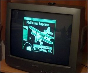
On the right is a video clip of my V2Z80P graphics system in action (apologies for dire capture quality).
Yep, a logo, starfield, some wibbly sinus sprites and a scrolly message, such were the things demos were made of in a time before polygons. There was no music in this early demo unfortunately, it just makes the classic phasing noise.
The intro weighs in at 15.5KB (uncompressed), there’s 8 hardware sprites (the wavey “PHIL2005” characters you can see there), 90 software sprite blobs – 30 on each bit plane, with a starfield on the 4th – both are double-buffered to avoid tears. I used hardware scroll and double buffering to assist the scrolling message – it moves at 4 pixels per frame so only needs to be byte shifted every other frame.
The old Z80 certainly requires you to jump through a few hoops to get the best speed – I didn’t use any self-modifying code, but had to unravel some loops and page align data tables to make indexing quicker (that’s one thing that’s sorely missing from the Z80 instruction set, a “Load r with (Address + Index)” – of course there’s the IX and IY registers but they’re slow as it is and the index is in the opcode which is inelegant to say the least). Also the software sprite routine is custom built for those 8×8 spot images and no pixel shifting is being done by the CPU – it just picks the a piece of code to run based the 3 Least Significant Bits of each blobs’ x coordinate and that code writes out a pre-shifted definition.
Incidentally, I use PASMO to assemble my Z80 code on the PC – an excellent and free util!
Soundcard..
My first attempt at a sound card was based on three PIC chips, each producing one channel of simple synth sound, it worked in a fashion but was cumbersome to update the sound channels, had untidy microcontroller code and was generally inelegant in design. Still, as a first try it could’ve been worse.
Originally the idea was to emulate the C64’s SID chip (here’s an interesting interview with its creator Bob Yannes) but the PIC microcontrollers I was using weren’t fast enough. The Ubicom SX28 with its 75MHz capability, on the other hand, would be. Simple waveforms like sawtooth, triangle and variable pulse could be generated using the phase accumulating oscillator principle (desc below) and white noise would just need a random number generator. In addition, sampled sound could be played using the the SX’s internal SRAM buffer with a Z80 interrupt generated every half-buffer period to get wave data updates.
A few sums revealed that 4 channels would easily be possible at a clock speed of 64MHz and these could be mixed digitally in the microcontroller. This would save having multiple R2R DACs and analogue mixing on the PCB. Also, as the SX has more ports than the PICs I was originally using, it would be easier to update the various sound parameters from the Z80 CPU.
One disadvantage in all this would be a drop in the “purity” of the sound output – the digital mixing would reduce the sound resolution unless I had greater than 8 bit output (which I briefly considered but decided it wasn’t worth the additonal external logic). In any case I guessed such issues wouldn’t be a huge deal – SID emulators on the Amiga always sounded OK after all (I wasn’t looking for anything like HiFi quality here!)
The Microcontroller Code
I designed my SX sound code to run on the RTCC interrupts at a fixed rate (I left the register update code running “in the background”). One channel’s output is calculated every interrupt and all four are mixed every forth to produce the final output for the DAC. The maximum interrupt frequency was arrived at roughly by measuring the longest path through the sound routine code and dividing by 4 (leaving some cycles over for the IRQ overhead and register update code to do its thing when needed). The simple waveforms only took a dozen or so clock cycles each, but they then needed to be scaled to control their volume. White noise was slower with the processing of a 24 bit linear feedback register (desc below) to provide the numbers. The sampled sound playing code took the most SX cycles due to it setting/caching internal pointers and creating the external signals for the Z80 IRQ side* The worst case (including scaling) was about 150 cycles per SX IRQ – but this still meant the SX at 64MHz could update its output at around 100KHz – more than double CD rate (but only 8 bit of course).
(* In my design only one channel can play interrupt-based sampled sound at a time in order to keep the interrupt signalling simple. With some more external logic all four channels could theoretically play IRQ-based samples – their buffer refill signals could set four flipflops and the OR-sum of those outputs would go to the CPU’s IRQ line. The CPU would then need to poll the flipflops to see which channel buffer needs new data. I think double buffering the channels in such a system would be pushing things a tad though, what with the SX’s limited SRAM).
As mentioned, the way I created the simple waveforms was to use a SID-like phase accumulator. In my case this was just a 24 bit counter to which I add a 16 bit value (directly related to the desired output frequency) each sample period. I then take bits 12-20 as my 8 bit output..
Osc hi:   Osc mid:   Osc lo:
=============================
00000000  00000000   00000000  <- Accumulator
              +
          Freq hi:   Freq Lo:
          00000000   00000000  <- Frequency control
----------------------------
    0000  0000
    !        !
    '--------'
         !
         '---------------------> 8 bit output
The raw output from the above would be a sawtooth shape, ie: rising and then suddenly dropping to the lowest point again. To make a triangle wave, I test bit 7 of the output and – if 1 – invert the other bits and shift it left. For a variable pulse width wave, I compare the output to an 8 bit pulse-width value held in a register, if it’s greater than this I set the output to the channel’s volume register and if lower, the output equals zero. This way, the pulse waves dont need any seperate scaling. For the white noise (and samples) I update the output if there’s any carry from the Osc_mid byte of the accumulator.
The linear feedback register used for the white noise is just 3 initially random bytes being shifted to the right with the MSB being fed the result of a XOR of various bits in the register.
>>>>>> Rotate Right >>>>>>
MSB                    LSB
00000000 00000000 00000000
!                   !  ! !
'----------<--------+--+-+   <- XOR'd bits
Volume scaling: There’s no divide or multiply instructions on the SX of course so my scaling routine uses the “shift and add” method (the equivalent to long multiplication by hand, in binary) to multiply the output by the volume to create a 16bit value, the most significant byte of the result is then the new output. Mixing the four channels is as simple as adding the four 8 bit outputs together and dividing by 4 (two right shifts). As the mixing only takes place every fourth interrupt, it occured to me that a digital filter could be implemented by dividing the difference between one output value and the next by 4 and using the result as a delta to modify the output EVERY interrupt and help smooth out the aliasing. The effect proved negligible though, I guess because the output was already being updated above 100KHz (and with sampled sound, the slope wasn’t between one actual sample and the next, just output updates). Anyway, the final value from the mixer routine is presented to an output port on the SX microntroller which is connected directly to a DIY digital to analogue converter – a simple “R2R” resistor ladder
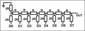
In a R2R resistor ladder, each output bit is connected to a series of resistors in such a way that each adds its binary weight to the total voltage at the end. From standard logic supply voltages, this gives a range of 0 to 5 volts in 256 steps (I used 10K and 20K resistors for my DAC – its not particularly critical). TV audio spec requires a 1v peak-to-peak signal, but its easy to scale it lower with a potential divider. I used a 50Kohm trimmer to set the level and buffered the output with a 7611 op-amp wired as a voltage follower. The output of the buffer is then just connected to the TV audio-in via a 1k resistor and 1uf capacitor.
My previous soundboard used a pretty slow method of sending data to the sound registers. This time all I do is latch (with 574 ICs) the Z80 databus and the high 8 bits of the address bus when I write to the sound port using the Z80 “OUT (c),a” instruction. (During this instruction, the Z80’s B register is presented to the high 8 bits of the address bus and the A register to the data bus.) Once these bytes are latched the SX can just toggle the latch chips’ output enables to get either the register address (for the SX’s FSR) or the data to place into it (mov to INDF). Sound board version 2. I also make any write to the sound port set a “busy” flag on a 74 flipflop and get the SX to clear it when the new data has been accepted. Any Z80 sound routine reads this flag through a 245 buffer before attempting to send any more data. Another line from the SX to the 245 buffer allows the Z80 to tell which half of the sample buffer is being used when playing digitized sound. The remaining bus lines of the 245 were pulled high via resistors and sent an (old) standard Atari 2600 joystick port:) SX28 source code is here. Click here for another badly scribbed schematic. Further reading / demo tunes etc can be found on this page
keyboard interface
A home computer without a keyboard is about as useful as a.. marshmallow crowbar? Anyway, as I didn’t want to build one from scratch this time the natural solution was to connect a standard PC PS/2 keyboard.. The internet again obliged with the necessary specifications for the PS/2 signals/protocol and the interface itself ended up consisting of another PIC microcontroller, a 74HC245 buffer and a 74HC74 flipflop to act as the “keycode ready” interrupt line. Minimal code was required for the PIC, it only needed to read the serial clock and data lines from the keyboard, convert the data to a scan code byte, present it to the 245 buffer and pulse a line to the 74HC74 to set the interrupt flag to get the CPU’s attention. 16f628 Souce code.
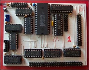
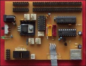
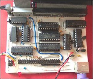
The PS/2 Keyboard Interface (and PSU) board The PS/2 keyboard I was using defaulted to “Set 2” scancodes on power up (most do, but I’ve since found a (USB) keyboard which does not initialize itself and needs to be told to manually reset..). As I didn’t need to send any data to the keyboard, it simplified the design a bit – it meant I couldnt control the caps lock LED etc, but I wasn’t too bothered about that. As mentioned I used a PIC to act as the keyboard interface – it buffered the PS/2 standard key/release scan codes and converted them to a custom system whereby just a single byte is sent for every key (I cared about) that was pressed or released (in my system, bits 0-6 hold the “set 2 scancode” AND $7F and bit 7 signifies press/release. The only key that could’ve spooned this up was “F7” which has the “make” scancode $83.. To stop any press/release confusion that code was trapped by the PIC’s software and converted to some other unused scancode before output.
The PCB shown was an early version with a 5 volt power regulator on the same board (mainly to use up the space). The keyboard interface eventually went on the same PCB as the IDE interface.
IDE Interface:
For storage, I thought about adding a flash memory IC (almost) directly to CPU address/data bus as I had some old BIOS chips recycled from PC motherboards that would have done the job. However they wouldn’t hold much data – half a meg – and the only practical “file system” would have been a very simple block save approach. I’d seen some 8-bit IDE interface circuits on the net, so I decided instead to implement that system instead – see this article.
File system:
With the IDE interface hardware and a couple of routines for basic sector access up and running, I started to think about implementing a file system. The possibilities ranged from the most basic “just save stuff to consecutive sectors and keep a list of filenames and a note to their start positions” to a full implementation of an existing file system such as Microsoft’s “FAT”. After looking into the FAT disk structure I decided it was too complicated for my purposes – I wasn’t interested in boot sectors, partitions and variable cluster sizes. At the other end of the scale, the simple “dump and tag” approach was a little too basic, what with its lack of directories (“folders” in MS-speak) and general organization. What I needed was a proper file system that would provide most of the functionality of FAT but without the unnecessary stuff.. so in the DIY spirit I decided to make my own..
Interlude – Some general filesystem background:
In simple terms, a file system is a software interface (or “layer of abstraction”) whereby files can be saved, loaded and deleted from a disk without the user having to worry about where the bits of the file are actually distributed – only a filename is required for access. In addition, a file system keeps track of which sectors are used and which are free as well as providing useful organisational features such as sub-directories. A file system divides up the storage area into “units of storage” and keeps a map of every storage unit on the disk, signifying whether it is empty / used / corrupt or whatever. PC hard drives inherently have sectors that are 512 bytes in length and these sectors are individually addressable – therefore the “granularity” is 512 bytes. In reality though you dont really want to individually tag each sector in your storage unit map: Modern hard drives have capacities of Gigabytes and to keep tabs on each 512 byte sector even on a 1GB drive you’d need 2 million entries in your map – pretty unwieldy! Instead, what happens is that file system creators clump sectors together into what Microsoft et al call “clusters” and each cluster is given an entry in the disk map rather than each sector. Upon formatting, the cluster size is set to an appropriate size dependant on the total capacity of the drive. The clusters are set as small as possible (so as to waste less space) – but there’s a limit to how many clusters can be addressed so the cluster size has to rise if the entire drive cannot be covered.
Meanwhile, back at the Z80 Project..
In designing my file system (which I called PQFS – “Phil’s Quickie File System”) I tried to keep things as simple as possible. I fixed my cluster size to 32KB (64 sectors – which I call a Block, just to be different) and there were other trade-offs like the area of the drive that the file system could “see” and the number of entries allowed in a given directory, but these things were unlikely to be too confining.
In PQFS there are three types of block:
Type 01 – The Block Allocation Table (The “BAT”)
Type 02 – A Directory Block
Type 03 – A File Block The first sector of each block is a header that shows what type each block is and holds information such as the file/directory name. The other 63 sectors of each block hold the actual data for that type of block.
Upon a PQFS format, the BAT block is saved at block location 0 (LBA sector 0), and the root directory goes at block position 1 (LBA sector 64). The first free block is at block position 2 (LBA sector 128).
Structure of each PQFS block type:
The BAT block:
Sector 0:

 Byte Offset:$00      - Ascii "PQFS"
             $04      - Block ID (01 = BAT)
             $05-$1ff - Not used for BAT

Sectors $01-$3f:

 $7e00 bytes, 1 per disk block with values:

             $00 = block is free for use
             $01 = block is in use
             $02 = block contains bad sectors
Directory Blocks:
Sector 0:

 Byte Offset:$00      - Ascii "PQFS"
             $04      - Block ID (02 = dir)
             $05      - Not used
             $06      - Parent Block (0 = root)
             $08-$0f  - Not used for DIR block
             $10-$1f  - This directory name in ascii (padded with spaces)
             $20-$1ff - Not used

Sectors $01-3f:

 Each sector contains upto sixteen of the following 32-byte entries, 1 entry
 per file or subdirectory. Therefore there can be a maximum of 63*16=1008
 files or sub-directories in any directory.

 Byte Offset:$00     - File / Directory name Ascii (padded with spaces)
             $10     - Attributes:
                                   Bit 0    : 1 = entry is a dir
                                   Bits 1-7 : Not used at present

             $11     - Not used
             $12     - Block location of named file / directory
             $14     - Length of file (not used if bit 0 of $10 = 1 (ie: a dir))
             $18-$1f - Not used
File Blocks:
Sector 0:

 Byte Offset:$00      - Ascii "PQFS"
             $04      - Block ID (03 = file)
             $05      - Not used
             $06      - The directory block that this file belongs to
             $08      - Next block in chain for this file (if length >$7e00 bytes)
             $0a-$0f  - Not used
             $10-$1f  - File name Ascii (padded with spaces)
             $20-$1ff - Not used

Sectors $01-3f:

 $7e00 bytes of data for file
Limitations of PQFS:
1. Only one block is allocated to the BAT and with one byte tagging each block, the maximum number of blocks that can be mapped is 63 * 512 = 32256. At 32KB per block the drive size is therefore capped at about 1GB (this could be easily expanded by using n-bit tags per block instead of a whole byte).
2. Only one block is allotted per directory. With each entry being 32 bytes, a directory can hold 63 * 512 / 32 = 1008 files (or subdirectories).
3. As the granularity is fixed at 32KB per block PQFS is wasteful, especially when used with smaller Compact Flash card and small files. Still, even a 16MB card could hold 500+ files or directories. What it does *not* limit is the size of files that can be saved (within the capacity of the disk of course:) File headers contain a file continuation link to the next block that contains data for a particular file (or zero if its the final block).
4. No checksums are implemented as yet – it totally relies on the hardware to report any faults. (There’s plenty of places checksums could be stored in the block headers)
File system procedures:
There’s number of key operations that are required for any file system: Format, Make directory, Delete directory, Change directory, Save file, Load file etc. Here I’ll give give a brief outline of the procedures I used to achieve some of them in PQFS (Naturally all these procedures should actually check that a disk is present (and PQFS formatted – except “Format” obviously) before doing anything.)
“Format”
Very straightforward: Create a blank, default BAT map (all blocks free except for the first and second blocks – ie: the BAT itself and the ROOT block below) and write it to block 0.
Form a new blank directory block called “ROOT” and write it to block 1.
(If you want to do a “long format” you typically fill each available block on the entire disk, check for bad sectors and make a note of them in the BAT).“Make a directory”
Scan the BAT for the location of the first free block, note its location (error if disk full)
Check that the required directory name doesn’t already exist in the current directory.
Scan the current directory block for a free entry space to place the required name and put it there. (Give an error if the directory is full)
Mark the free BAT location found at the start as taken.
Create the header sector for the new directory.
Write the header sector to the appropriate location.
Zero the rest of the sectors in this block“Change directory”
A file system can create the impression of branching tree of subdirectories by simply having a variable that holds the block position of the the current directory. When you change directory, the pointer is updated to the block location of the specified directory name. The “parent directory” function is achieved by updating to a pointer from the header of the current directory block (which was placed there when the directory was created.)
To change directory you’d do the following:
Scan the curent directory block for a match to the name specified. Error if not found.
Check the attributes of the match found – is it in fact a file not a dir? Error if apt.
Copy the matched directory’s location pointer to your current directory block variable.
(To move “up” a dir – check if the filename is “..” (or whatever) and update to the “parent block pointer” held in the header of the current directory block, giving an error if its already at the root directory).“Delete a directory”
This isn’t as straightforward as you might first think. If you simply remove the directory name entry from the current directory block and a free up it’s block in the BAT, all the files and subdirectories that may have been in that directory will become “lost” but will still take up disk space. You therefore have two options, a) step through the entire sub-directory tree, deleting everything as you go.. or b) only allow empty directories to be deleted, forcing the user to do the donkey work.. I did the latter :)
Scan the current directory block for a match to the name specified, error if not found.
Check the attributes of the match found, is it in fact a file not a dir? Error if apt.
Move to the block position of the directory match and check its entry list to make sure the directory in question is empty. Error if it contains stuff.
Go back to the current directory block and delete the unwanted dir entry.
In the BAT, mark the block position previously used by the directory as free.“Save a file”
The operates much like the procedure for creating a directory, with the added complexitity of linking blocks for files longer than 63 * 512 bytes.
Scan the BAT for the location of the first free block, note its location (error if disk full)
Check that the required file name doesn’t already exist in the current directory.
Scan the current directory block for a free entry space to place the required name and put it there. (If the directory is full -> error.)
Mark the free BAT location found at the start as taken.
Create the header sector for the new file.
Write out the header sector to the appropriate location and fill the block’s following sectors with bytes from the file. Stop when all bytes written or the block is full.
If all bytes have been saved, end the procedure.
Scan the BAT for another free block, note its location.
Mark new BAT block taken.
Update the “continuation pointer” in the header of the previous file block to point to the new block
Create a header sector for this next block.
Go to to step 6“Load a file”
Normally it’s best to break up this procedure into two seperate routines. The first being “Open file” (which checks for the existence of the file etc) and the second “Get file data” (which actually loads in the data). This means that programs can get information about a file without actually loading the whole thing, plus you can modify the information that “Open file” produces to truncate the file length etc.
“Open File”
Look for a match of the required file name in the current directory block (error if not found)
Check that the entry is a file and not a directory (error if a dir).
Note the starting block of the file.
Load the header sector of the file and note all relevent info; file length etc.“Get File Bytes”
Obviously dont procede if “Open File” failed.
Move to the block addresses saved by “Open File”
Load in data bytes from the block to memory, decrementing the “file length” variable created by “Open File” as you go.
If you reach the end of the last sector of the block before “file length” = 0, read in the header of this block and obtain the file continuation block address.
Move to the new block address and goto step 3“Delete a file”
Like “delete a directory” except you must follow any continuation links and free up their blocks in the BAT too.
Scan the curent directory block for a match to the name specified, error if not found.
Check the attributes of the match found, is it in fact a directory not a file? Error if apt.
Make a note of the file’s start block.
Delete the unwanted directory entry.
In the BAT, mark the block position previously used by the file block as free.
Check the header of this block for a continuation link. End if it is zero.
Goto step 5, using the continuation link just found as the file’s block position.And essentially, that’s my quickie file system. Obviously it could be greatly improved but as I say simplicity and compactness were my goals.


