-
An 8-bit IDE interface
Although there are now technically simpler storage options for hobby projects, the 40 pin ATA IDE interface is still a ubiquitous, well documented connector which allows hard drives and Compact Flash cards (via a simple adapter) to be used. The only real complication is that ATA IDE has a 16 bit data bus, so an interface must be made in order to connect devices to 8 bit systems.
The IDE connector pin-outs:
/Reset	-  1  2 - Ground
Data7	-  3  4 - Data 8
Data6 	-  5  6 - Data 9
Data5 	-  7  8 - Data 10
Data4 	-  9 10 - Data 11
Data3 	- 11 12 - Data 12
Data2 	- 13 14 - Data 13
Data1 	- 15 16 - Data 14
Data0 	- 17 18 - Data 15
Ground 	- 19 20 - No pin (Key)
DMARQ 	- 21 22 - Ground
/Write 	- 23 24 - Ground
/Read 	- 25 26 - Ground
IORDY 	- 27 28 - CSEL (Cable select)
DMACK 	- 29 30 - Ground
IRQ 	- 31 32 - Obsolete: no connection (formerly "IOCS16")
Addr1	- 33 34 - PDIAG / CBLID (UDMA detect)
Addr0 	- 35 36 - Addr2
/CS0	- 37 38 - /CS1
DASP	- 39 40 - Ground
All pins are TTL compatible, control signals are active low. (Note about using Compact Flash cards in “True ATA mode” via IDE adapters: According to the spec sheet, these cards require CMOS level logic inputs – so when running with Vcc at 5 volts, logic highs should be a minimum of 4v. This wont be an issue using 74HC series logic from a 5 volt system such the Z80 but its worth bearing in mind if mixing logic families etc.)
Pin Descriptions:
Data 0 – Data 15: The 16 bit bidirectional data bus
Addr0 – Addr2: 3 bit address bus (inputs)
CS0 & /CS1 – Chip Select inputs (gates the device onto the bus)
/Read & /Write – input (pulse low with Address steady and Chip Select low to read or write)
/Reset – (input) reset the drive’s hardware,
The “DASP” pin is open collector and can be used as a drive activity indicator when connected to a LED from Vcc via a resistor.
Most home-brew IDE circuits I have seen leave the DMARQ, DMACK, IORDY, PDIAG, CSEL and IRQ lines nconnected, however the following may be worthy of note:
DMARQ is an output from the drive used in high speed DMA transfers so presumably can be ignored.
DMACK is an input at the drive used to acknowledge DMA mode – I noted that the Compact Flash ATA mode spec sheets say if there is no DMA-mode ability in the host (as there wouldn’t be for a simple interface) DMACK should be driven high.
IORDY is an output from the drive which can be used to slow down read/write cycles if they are too quick (ie: insert wait states) I have not used this signal. The ATA spec sheet suggests it be pulled high with a 1k resistor min (presumably, that’s only if it is to be used by the host circuit.)
“CSEL” is used for “cable select” of master and slave drives when using a special cable. In Cable Select mode, drives pull their CSEL inputs up via a 10K resistor, and this signal can pull the input down to Ground (so at the host end CSEL should be grounded). “Cable Select” IDE cables have the CSEL conductor cut beyond the the first drive connector on the lead, this way the first device sees itself as the master (pulled down to Gnd) and the second sees itself as slave (not pulled down). If in doubt use the Master and Slave jumpers on the drives, this line then become irrelevent.
Interface requirements:
IDE devices are accessed via 16 registers which you read and write to just like normal memory locations. Certain registers accept commands (eg: “read sector”) others report error status flags etc. Most of the registers can be thought of as 8 bit bytes as only D0:D7 return and accept useful data. It is only data being read from or written to the disk that is transferred as 16 bit words (there’s more detail on this below). The two chip select lines activate a different set of registers: When /CS0 goes low, registers 0-7 are accessed, and when /CS1 goes low 8-15 are accessed.
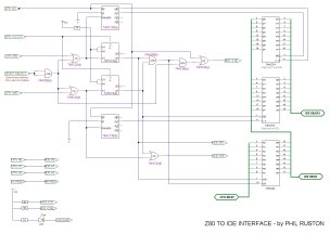
A basic 8 bit interface must handle the 16 bit databus, a 3 bit address bus, 2 chip select lines, /Read & /Write lines. (/Reset can be tied to the host system’s reset line) To convert 8 to 16bit you can use two 8 bit latches, one for outgoing data and one for incoming data. When reading the low half of the IDE data bus, the high 8 bits can be latched, you can then read the contents of the latch afterwards. When writing, you write the high byte to the other 8 bit latch, and this byte is presented to the high part (D8:D15) of the IDE databus when you write the low half (D0:D7) directly. It’s probably best to also include a bus-transceiver (EG: 74HC245) in the interface to provide a single load point to the host’s databus, it isn’t absolutely necessary though.
The address lines A0:A2 can be routed directly from the host to the IDE bus or latched (which would mean a little more read/write preamble in your driver software). The IDE chip select lines /CS0:/CS1 need to be decoded from the host’s address bus and port enable line (EG: Z80’s /IOREQ) Tip: You typically dont need to access IDE registers 8 to 15 so /CS1 can just be pulled high via a resistor. Alternatively /CS0 & /CS1 can be latched (eg: in the same IC as the address lines A0:A2).
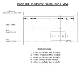
Depending on how you handle the IDE chip select lines, /RD & /WR can be routed direct from the host’s processor or via decoding logic. More logic is required to operate the latches’ clock pulses and output enables appropriately and to decode the port address mapping the IDE interface into the processor’s address space. Timing is important, you want the IDE /WR and IDE /RD lines to pulse low whilst the IDE chip select signals (/CS0 or /CS1) are stable and active.
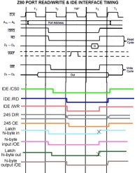
Also, if writing through a bus transceiver, you need to ensure its outputs are enabled and the data direction remains stable until after the /WR line has gone high. Such timing can be achieved asynchronously by utilising the propagation delays associated with logic gates. A more reliable approach is to use the host’s CPU clock and D-type flip-flops to keep things in check.
My own Z80 IDE interface (shown above right, which I’ve tested up to 8Mhz so far) was based on 7 discrete logic chips (74HC245 bus transceiver, 2 x 74HC574 8bit latch, 74HC139 dual 2-to-4 line decoder, 74HCT08 quad AND gate, 74HC32 quad OR gate, 74HC74 dual D-type flip flop). It uses the Z80 clock signal and some flip flops to ensure the various chip outputs are left open at the correct times (see diagram on the right). The address lines are unbuffered and I’ve used the Z80 address line A3 to dictate whether access is being made to the low half of the IDE databus or the high (IE: the latch ICs). For example: if I mapped the IDE system to port range $40-$4F and wanted to send $1234 to the IDE device I would use:
ld a,$34
out ($48),a ;”pre-write” high byte to latchld a,$12
out ($40),a ;write low byte (high byte presented from latch)(Incidentally, the “pointless” first AND gate in the schematic acts simply as a LVTTL->CMOS level converter (I used a 74HC*T*08 chip). This is because my port decode signal was sourced from a 3.3v FPGA IC.)
Software: Simple IDE driver
The ATA protocol has been expanded to very complicated levels over the years but the drives still run fine on the default non-DMA modes (ie: mode0 to mode6.) Access can be pretty straightforward: You tell the device the sector number you want to access, give it a command and then transfer the data, checking status flags at the appropriate times.
Here’s a run down of the IDE registers accessed by A0-A2 and /CS0 & /CS1 – some simplifications have been made. EG: I’ve ignored all the old head/cylinders/sectors way of addressing sectors as that’s ancient history. Using the LBA (Logical Block Address) mode is way more logical: Each sector is simply addressed sequentially, via the 28 bit address held in registers $3-$6 (Incidentally, this is where the pre-LBA48 137GB drive size limit comes from in Windows: 2^28 sectors * 512 bytes = ~137GB)
IDE reg: A0-A2: /CS0: /CS1: Use:

  $0	000    0    1     IDE Data Port
  $1	001    0    1     Read: Error code
  $2	010    0    1     Number Of Sectors To Transfer
  $3	011    0    1     Sector address LBA 0 (0:7)
  $4	100    0    1     Sector address LBA 1 (8:15)
  $5	101    0    1     Sector address LBA 2 (16:23)
  $6	110    0    1     Sector address LBA 3 (24:27) (also see **)
  $7	111    0    1     Read: "Status", Write: Issue command to drive
  $8	000    1    0     Not Important
  $9	001    1    0     Not Important
  $A	010    1    0     Not Important
  $B	011    1    0     Not Important
  $C	100    1    0     Not Important
  $D	101    1    0     Not Important
  $E	110    1    0     Not Important
  $F	111    1    0     Not Important

** Bits in register $6:

Bit 0:3 = LBA bits (24:27)
Bit 4   = Select Master (0) or Slave (1) drive
Bit 5   = Always set to 1
Bit 6   = Always Set to 1 for LBA Mode Access
Bit 7   = Always set to 1
Some detail:
Register $0 is the 16 bit data register. You read and write sector data words to and from this address.Register $1: Can be read for more detail when the ERR (bit 0) in STATUS (reg $7) below is set:
Bit: Condition:

 0    1 = DAM not found
 1    1 = Track 000 not found
 2    1 = Command aborted
 3        Reserved
 4    1 = ID not found
 5        Reserved
 6    1 = Uncorrectable ECC error
 7    1 = Bad block detected
Register $2 holds the number of sectors you want to transfer in one go, typically 1.
Registers $3 – $6 hold the address of the sector you want to access (see note about register 6)
Register $7 accepts commands when written to and reports the drive status when read.
IDE Register $7 WHEN WRITTEN = Send command to drive.

Some key commands (there's loads more besides) :-

$20 - Read sectors with retry
$30 - Write sectors with retry
$EC - Identify drive

IDE Register $7 WHEN READ = drive status:

Bit: Name: Condition:

 0   ERR    1 = Previous command ended in an error
 1   IDX        (not important)
 2   CORR       (not important)
 3   DRQ    1 = Data Request Ready (Sector buffer ready for transfer)
 4   DSC        (not important)
 5   DF     1 = Write Fault
 6   RDY    1 = Ready for command
 7   BUSY   1 = Controller is busy executing a command.
Sending commands
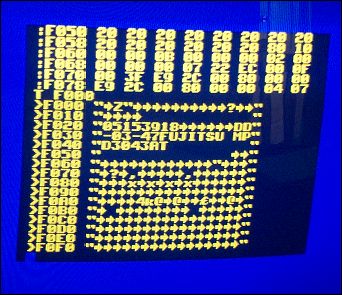
The “Identify drive” command is useful as it tells you your interface is working (without having to read anything from the disk itself). The command returns 256 words of data containing a lot of info about the connected/selected drive including the device name in ASCII (40 chars @ byte offset $36) and the capacity of the drive in sectors (2 words @ byte offset $72, least significant first).
The procedure for getting a drive’s ID is:
1. Make sure BUSY=0 and RDY=1 before proceding.
2. Select the drive master/slave with appropriate write to IDE reg $6.
3. Send “Drive ID Command” ($EC) to Command Register $7
4. Wait until BUSY=0 and DRQ=1
5. Check error flags.
6. Read 256 words from data port 0.
The procedure for reading a sector is:
1. Make sure BUSY = 0 and RDY =1 before proceding.
2. Tell the drive what sector is required (fill in the LBA address regs)
3. Set number of sectors to transfer to 1 (reg $2)
4. Issue read sector command ($20) to reg $7
5. Wait until BUSY=0 and DRQ=1
6. Check error flags.
7. Read 256 words from data port 0.
The procedure for writing a sector is:
1. Make sure BUSY = 0 and RDY = 1 before proceding.
2. Tell the drive what sector is to be written (fill in the LBA address regs)
3. Set number of sectors to transfer to 1 (reg $2)
4. Issue write sector command ($30) to reg $7
5. Wait until BUSY=0 and DRQ=1
6. Write 256 words to data port 0.
7. Wait for BUSY to become clear and RDY to become set.
8. Check error flags.

Bytes from the 'Get ID' command. Note the drive name.
A note about byte ordering: When you read the words from the IDE device and copy them to your sector buffer you can chose to order them in big or little endian byte format. If you store them in a little-endian system (Z80, Intel) then the ASCII characters from the Get ID command will be out of sequence because the IDE specifications dictates that the ASCII bytes in the Device ID “sector” are interpreted with the high byte as the first character of each pair. IE: (Word N) “bits 15:8”, “bits 7:0”, (Word N+1) “bits 15:8”, “bits 7:0” etc etc.. In my IDE code, I save the words big-endian style as a simple way to avoid this, but it does mean that if you use my code to read *actual data sectors from existing file-systems*, each byte pair will appear switched around. Well, that’s about for the basics of reading and writing to an IDE drive a sector at a time. Here’s the core Z80 source code I programmed to operate my Z80 interface. There’s no warranty and it may have bugs (though it works OK for me:) “Educational use only!” as they say..
Notes:
This kind of interface is ripe for integration into a CPLD / FPGA etc – but beware of voltage levels and ground bounce issues. EG: I once had major problems with a glitch on the /CS0 line causing random double clocking when transferring the data words from sectors. Also note that the above interface, based on discrete logic relies on the propagation delay of 3 gates to seperate /CS0 and /RD going inactive (t9). On a CPLD/FPGA you cannot
rely on such things.File systems: If you need to load and save real files and not just log sectors, you will of course need a file system. The FAT file system is reasonably well documented on the net or you could do what I did and make your own (see the Z80 Project)
Further Reading:
CompactFlash.Org – Specs available for download etc
Peter Faasse’s 8255 to IDE interface
Compact Flash to IDE adapters on ebay UK
Official ATA specs – very detailed (too much so in fact)


