-
V3Z80P
System Board..
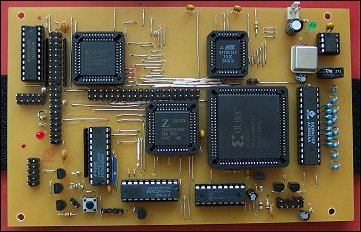
The V3 Z80 system board replaces three PCBs used previously. The functionality remains largely the same, but some optimizations have been made; CPLDs used to replace discrete logic chips and surface mounted components used here and there to save space. Pin headers have been used so that flat cables with IDC sockets can lead out to the final connectors.
One of the optimizations concerned the Z80 memory mapping which was changed to best utilize a single RAM chip (an SMT 128KB, 70ns async SRAM) for all the RAM requirements. In the Z80 address space, $8000-$FFFF is paged so that three sections of memory can appear in those locations (banks beginning at $8000, $10000 and $18000 in the actual SRAM), with the banks being selected by a couple of bits in a port register of CPLD #1. Z80 address space $800-$7FFF is fixed to $800-$7FFF in the SRAM and $0-$7FF selects the boot ROM IC (a more flexible system would’ve allowed the boot ROM to be switched out totally but it as it contains the font also used by the OS, it didnt waste much space).
There are two CPLDs taking the place of a lot of the discrete logic, their functions are:
CPLD #1 – XC9572 (15ns): Decodes address lines to provide chip select signals for the RAM and ROM. Holds port output and control registers and demultiplexes address lines to select them during OUT instructions, allows data from input ports onto the Z80 databus during port read (IN) instructions, masks and ORs together incoming interrupt lines from video, keyboard and the sound, acts as interface to SX28 sound system (latches data written by Z80 until the SX28 is ready to accept it).
CPLD #2 – XC9536 (15ns): IDE interface: presents a 16 bit word to the IDE databus following two 8-bit port writes and presents the 16bit word to the Z80 in two byte chunks during two port reads. Uses an external bidrectional 8-bit buffer IC (74LS245) to sit between the low 8 bits of the IDE databus and the Z80 databus – provides select and data direction signals for this IC.
The two microcontrollers on the board have the following functions:
Microcontroller #1 – PIC16F627: Keyboard interface (Uses internal RC clock gen @ ~4MHz) Talks to a standard PS/2 PC keyboard in serial format and presents the keycode data as bytes to a 8 bit buffer IC. (A line from CPLD #1 allows its data onto the Z80 bus during the approriate port read.) Also produces a system wide reset pulse and NMI for the Z80 in response to a sequence of keypresses. Described in detail elsewhere.
Microcontroller #2 – SX28 @ 64MHz. 4 channel sound system. Accepts data from CPU via CPLD #1 and produces tones and simple waveforms. Channels are mixed digitally and output fed into an R2R resistor DAC. Described in detail elsewhere.
Graphics PCB..
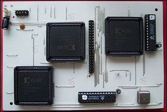
To condense the discrete logic of my graphics system onto a single PCB I used three CPLDs – flash programmable chips that can take on the function of x number of logic gates. Ideally the entire glue logic of the graphics system would go on one chip but there were too many gates to fit in the kind of CPLD I was using, ie: affordable, PLCC socket types. (There are of course FPGAs which would hold the entire project – but they have many additonal complexities and I was taking it a step at a time and using CPLDs)
When deciding how to spread the logic over the three CPLDs, I largely stuck to the way the functions were arranged across the PCBs of the V2 system. Having said that, most of the actual logic was totally redesigned. The biggest change was the removal of the 2nd parallel display buffer from the original design – its original purpose was to allow the CPU to read/write a display buffer at full speed all the time (a bit like dual-ported RAM) – however it was cumbersome, doubled up a lot of logic and didnt really justify itself in terms of performance gain, so I ditched it.
Anyway, here’s a run down of the functions assigned to the CPLDs (the actual schematics can be found in the file base)..
CPLD #1 XC95108 – Handles switching the address bus of the video ram SRAM between the CPU and the video system. Also contains the address counter for the video system (which now has two modes of operation for bitmap and character map modes) and the planar-to-chunky pixel converter. Interfaces with SX28 which organises pixel datafetch.
CPLD #2 XC95108 – Is the main interface to the Z80, contains the video registers and memory address range decoding. Has logic to generate the video frame timing (this is new in the V3 system, previously the TV frame was handled by a SX28 microcontroller).
CPLD #3 XC9572 – Sprite and Palette control. Switches address bus of sprite SRAM and palette SRAM between the Z80 and video system. Interfaces with SX28 sprite controller.
The system still utilises two SX28 microcontrollers (clocked at 64MHz) but the function of the graphics controller is now different.
SX28 #1 – Main graphics control. Originally I was using this to generate the TV frame timing but that is now handled by CPLD #2 in pure logic. This microcontroller now clocks data into CPLD #1’s planar-to-chunky shift registers during the horizontal off-screen raster time, accepts the rearranged data back from the CPLD, and builds up a line of 256 4-bit pixels in its internal SRAM which it clocks out during the on screen raster time period (in sync with the sprite controller). The firmware of this microcontroller is also responsible for horizontal hardware scroll, which is merely a delay of 0 to 7 pixels when dumping out a scan line.
SX28 #2 – Sprite controller/generator. No major design changes since verison 2, just performance improvements really. Reads coordinate/definiton data from the sprite SRAM, organises it into a pre-built scanline of 256 4 bit pixels and dumps it out in sync with the background video data.
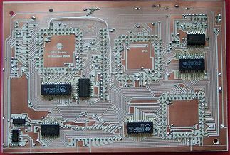 The graphics system uses three 5-volt async SRAM memory chips. Naturally it’d be elegant to have everything on one chip, but still..
SRAM #1 – Bitmap data: 128KB ~12ns SRAM.. Connected to CPLD #1 – Holds four banks of 32KB video data, each enough for a 16 colour 256 x 200 pixel display or four banks of two 256 8×8 16 colour characters sets and two 32×25 character maps. Needs to be high speed RAM so the SX28 can build the scan line during offscreen raster time.
SRAM #2 – Sprite data: 32KB ~12ns SRAM. . Connected to CPLD #3 – Holds upto 253 16×16 16 colour sprite definition blocks (first two blocks contain coordinate data etc) Again, needed to be fast SRAM so the SX28 could build a scanline containing at least 8 sprites in the allotted time.
SRAM #3 – Palette: 32KB ~70ns SRAM – Connected to CPLD #3 – Capacity was overkill as I’m only using 256 bytes – there was no price advantage using a smaller IC however. The background bitmap has a 16 colour palette and the sprites have a 16 colour palette (15 plus transparent) – which of course adds up to 32. However, its easy to just supply the SRAM address lines two groups of 4 bits and set the 256 colour registers to compensate – this also allows crude semi-transparent effects etc. The slower 70ns SRAM is sufficient as my pixel clock is only 125ns.
The other chips used are:
A 74HCT541 tri-state buffer to switch the Z80 databus to the sprite SRAM (single direction as the sprite SRAM is write only as far as the CPU is concerned)
74HCT245 bidirectional buffer to switch the Z80’s databus to the video SRAMs (bidirectional, as the CPU needs to read and write from video memory)
74HCT574 octal latch (output buffer to an R2R resistor net colour DAC).
74HC04 hex buffer/inverter and 74HC4029 divider used to distribute an 64MHz oscillator’s output to the two SX28s and divide down to 8MHz for the Z80 board and video clock.
Sound tweaks..
I’d hadn’t really done much with the soundchip since version 2 of the Z80 Project – even then I’d only had it produce a few test beeps. Ideally I wanted it to play music – not the latest bangin’ mp3s of course (its soooo not capable and well, that would be dead boring and un-retro anyway:) No, music as in 80’s / early 90’s game tunes! I’m absolutely *not* a musician myself so I needed it to play existing music files – the most usable and readily available being Amiga Protracker modules (I couldnt really use C64 SID tunes as there’s no standard replay routine, PC players have to emulate the C64’s CPU as well as the sound hardware). So… there was my challenge, write a Protracker replay routine in Z80 that’d work with my hardware.
Slight snag: the Amiga’s sound hardware is a 4 channel sample player and my soundchip is more like a 4 channel version of the C64’s SID chip, ie: a tone generator. It *can* play sampled sound using interrupts but due it only having a 64 byte internal buffer and no DMA abilities, it can only manage one sampled voice at a time. Some dodgy multiplexing shennanigans could’ve had it playing x sampled voices of course but that would hog the CPU and be useless for games and demos. Clearly another approach was required.
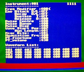 I decided to try to strip out the sample data from the Protracker modules and only use the note/fx sequence data. I then could synthesize voices in software to approximate the original samples. With a software voice generator I figured it would be perfectly adequate for “chip tunes” (small modules with simple waveforms as samples). This wouldnt need to be very complicated: a wide variety of voices would be generated by modulating the pulse width of the square wave generator, rapidly switching wave types, creating an envelope to add shape to the sounds etc. Each voice would be numbered and triggered using the data that the Protracker replay routine would normally be sending to the Amiga’s hardware registers. And so I set to work (whilst I was at it I made a front end for the wave editor, shown in the pic on the right).
The first tune I converted was one I’d used in Giddy3 as the game completion tune (called Skogen’s Djur 20 written by Daniel Johansson) – I’ve put an mp3 of the Z80 project playing it below. Its a nice crisp tune that doesnt use anything too fancy in terms of waveforms – it came out quite well I think.
Some of the tunes I tried next had distinctive sounding wave shapes and I was having trouble matching them accurately in software so I had another think about playing digital sound. As the waves for such voices were really tiny (about 32 bytes) I realized I could download them to the SX28’s internal SRAM (I had 64 bytes to play with -woo!) when the parent module was initalized. From there they could be played by all 4 channels at once if required. So, a new wavetype was added to the soundchip firmware: “Play sample loop from internal registers” – some pointers to the start and end locations were required and then away it could go just like any of the synthetic waveforms.
Whilst I was looking into this I remembered how the SID chip did “ring modulation” effects by flipping the output of the triangle wave generator based on the square wave output of another channel (ie the MSB of another channel’s accumulator), its probably not going to be much use for music but it makes some interesting FX so I implemented this wave type too.
The SX28 has 2048 12-bit locations that can be used for its program. My sound firmware had used about 500 of these words and I wondered if I could employ up the rest usefully. Most modules use drum sounds, so I decided it’d be a reasonable idea to put a micro drumkit in there: a bass drum, a snare and a hi-hat would just about fit with some radical downsampling and 6-bit conversion – and hopefully still sound like drums :) The SX28 IREAD instruction made it easy to read the program word locations as data so I wrote a small routine in Pure Basic to convert the samples to source code and included them as data in the SX28 program. Of course the sounds can also be chopped and mixed by the synth code just like the other voices so a variety of FX can be spawned from the raw samples.
Here’s some mp3s of protracker chip tunes I converted:
- Skogen’s Djur 20 (196KB MP3) (Module By Daniel Johansson)
- Monty O.T.R Hi Score (1.3MB MP3) (Original tune by Rob Hubbard, Protracker version by dreamfish)
- Her Numbness (943KB MP3) (Original module by estrayk ^ paradox)
- Monday (543KB MP3) (Original module By Random Voice)
- Skogen’s Djur 8 (450KB MP3) (Original module By Daniel Johansson)
- Hawkeye Highscore (524KB MP3) (Original by Jeroen Tel, Protracker vers by Pink of $ceptic/Abyss
Serial Comms..
Originally I was using a couple of parallel port bits to transfer data serially to and from the from the Z80 project. This meant I had to use a custom data server program I’d written which only worked reliably in DOS (cus I could switch the PC’s interrupts off, essential for accurate timing). What I really needed was a Windows app using a standard RS232 serial connection. This required two things: a) A small interface circuit to convert the RS232 voltages to 5 volt logic and b) A serial file transfer program.
The interface:
The interface circuit was quite simple – I used a MAX232 IC to convert the RS232 signal levels and a PIC16F627 to buffer and relay the data. The PIC wasn’t absolutely necessary but as it has a UART built in, it saved me worrying about exact timing at the Z80 end. Useful, as even with this new RS232 serial system, the Z80 project is still sending and receiving data via its simple 9-pin Atari 2600 style joystick port (no interrupts, its a simple CPU hogging affair to send and receive. I could’ve tried to implement my own hardware UART in the main Z80-facing CPLD but.. well, didn’t..:)
The joystick port has 6 input lines.. Normally these are for the 4 directions and two fire buttons but here 4 inputs are used to receive a byte from the PIC in two 4-bit chunks. One more bit is used for a clock signal and the other input is for flow control between the PIC and the Z80 project (tells Z80 side not to send any more bytes until this current one is passed on). The clock is a DDR type arrangement, the first part of the byte is presented to the 4 inputs when the clock goes high, the second part on clock going low.
When sending data to the PIC (for relaying on to the PC) data is sent using two spare pins (clock and data) in the 9-pin joystick connector (which are configured as open collector port ouputs on the Z80 project’s PCB). The PIC s/w arranges the bits received into the original byte before putting it into its internal serial-out h/w register for transmission to the PC.
Note: I haven’t used any actual RS232 hardware flow control on the PIC-to-PC side, its just a 3 wire “TX, RX and Gnd” connection.
PIC software:
The PIC software is very simple. It waits for either of two conditions:
a) Its internal h/w register has received a data byte from the PC side.
b) The Z80 side wants to transmit a byte.In the case of a) the PIC clocks out the byte from the PIC’s hardware serial input buffer to the Z80 side in two chunks as mentioned above.. This happens sooner than two sucessive bytes can be received at the fastest allowable baud speed (so there is no need for flow control this direction.)
In the case of b) the PIC sets the wait (flow control) line, listens for 8 serial bits from the Z80, puts the byte into its hardware-out register, sets it to transmit, waits for it to be sent then clears the wait line.
Transmission speed:
The Z80 side does not need to know the RS232 baud rate (the Z80 communicates with the PIC as quickly as it can/is reliable). The PIC and PC side software must agree on the baud rate. The system is set up to work from 9600 to 56700 baud (the PIC PCB has jumpers to set the speed).
PC Software:
I was able to test the circuit and Z80 side software by using HyperTerminal in Windows. HyperTerminal also allows files to be sent using protocols like X-modem, Z-modem etc but when I looked deeper into these, they all turned out to be either too restrictive (X-modem’s 128 byte “granularity”) or overkill (Z-modem’s compression etc). I decided I needed to write my own file transfer program.. The problem was finding a way to access the serial port easily – AFAIK modern Windows variants do not allow direct low-level access to the hardware ports, so a simple DOS program was out. Fortunately I’d recently been looking at Pure Basic (a great straightforward version of BASIC, which makes nice small executables). With it I was able to make a small util to send and receive binary data from the Z80 Project over a true serial link.
A demo!
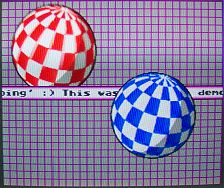
This demo was done to test out two of the new features of the V3 Z80 project; the enhanced sprite controller and character mapped display mode. Click the pic on the right to play the video (2MB – divx .avi)
Technical details: The demo runs at 50 frames per second (naturally:) but my crumbly video capture card / camcorder combo would only allow me to do a 25 FPS avi. There’s also no tearing in the original, the split you may see on the video rolling down the screen was caused by the camcorder being slightly out of sync with the TV.
Really technical details: The display is actually in character mapped mode. The blue ball is made of hardware sprites and the red one is actually “the background” (using a character set made of ball fragments) which is being shifted smoothly with hardware scrolling. The grid behind both balls is regenerated each frame (its all the same character:) to compensate for the scrolling. The edge characters of the red ball also have to be regenerated each frame to cleanly mask the ball against the “changing but stationary” grid. The scrolly message uses a similar scroll compensating method along with beam sync’d IRQs and colour bars. Phew!
The tune is originally from the C64 game Hawkeye. Here the Z80 project is playing an Amiga Protracker conversion which I converted to use synth instruments (again) with my sound editor – kinda full circle, no? :)
You can download the files for the V3 Z80 Project… here.


